

Technical Basics
Semiconductor devices - Diodes
2I1 Recall that a diode will conduct current in one direction only.
Let's take a step back and discuss for a moment conductor and insulators. Conductors are materials that have free electrons and insulators are those materials which have no free electrons.
We are now going to move onto a material that is partially conductor and partially insulator and it is called a semiconductor.
The circuit diagram for a diode is :-
 also called a junction diode.
This component is part of a group of components that use the special properties of materials called "semiconductor" mentioned above to control the flow of electrons (others in the group are transistors, mosfets and leds (light emitting diodes).
The diode is made up of two distinct parts an "N" type material which has excess of electrons and "P" type material which has a lack of electrons. These two piece of material are joined together and there is the junction between the two materials and hence the name JUNCTION DIODE.
![]()
This concept of P and N type semiconductor materials will be used again in the transistor section further on.
The diode only allows a flow of electrons in one direction and thus a current will only flow in one direction. As you learned in the foundation Course the conventional current flow, or just current flow, is in the direction of the arrow ( but in actual fact the electrons would be flowing the opposite way).
If this is confusing then think only in terms of what we have called converntional current flow and that is in the direction of the arrow head so the arrow head would be positive and this is shown in the diagram below.
As you never obtain something for nothing, for the action of the diode to take place there is a need for a small forward potential (also called forward bias or turn on voltage) to "turn" the diode on. What this means in real terms is say there is a 12V potential prior to the diode then afterwards there would be of the order of 11.4V, 0.6V being the "forward potential".
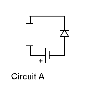
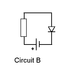
From the circuits drawn above will current flow in circuit A or B.
Here you will have to determine which is the + positive side of the battery and thus recall that it is the "longer" side of the battery symbol.
Conventional current flow, and that is the one we all now talk about, is from Positive to negative.
So if you wanted to determine what current is flowing in a circuit through a resistor you must first confirm that a current is in fact flowing, particularly when there is a diode in circuit. So check the current flow from positive to negative is flowing through the diode which is in the direction of the arrow ( meaning the shape of the diode symbol ! ).
Thus looking at the circuits above you can now determine that only in Circuit B does the battery provide the flow that will pass through the diode and a current flow occur.
So if you were shown the diagram of Circuit A there is no flow of current so on an ammeter you would have a reading of 0 Amps !!!
Understand the use of a diode to produce direct current from an alternating current is known as rectification.
Earlier it was have explained that the AC that leaves a transformer's secondary winding. This AC is of very little use except to say light a torch bulb, as most electronic equipment required a source of DC.
From above you have seen how the "diode" can be used to make sure that the current only flows in one direction. Thus when a diode is added to the transformer circuit it can change the AC into DC by suppressing the flow the wrong way.

The basic transformer and no other components
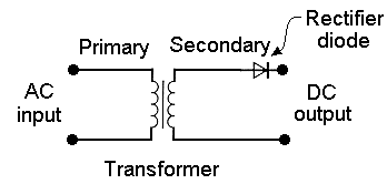
The output only becomes DC due to the Diode, if the diode was removed the output would again be AC
If you have an AC source and want DC then use a rectifier diode
Above right the simple circuit represents the transformer with the primary and secondary winding (coils / inductors) and a single diode.
Whilst the output from the transformer prior to the diode is still AC the transformation from AC to DC is called "rectification" and in the case of the single diode is called "half wave rectification" as only half the AC waveform is doing any useful purpose.
You could say that the AC pulses have been converted by the diode to DC pulses.
Identify the AC and rectified (pulsed DC) waveforms.
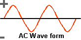
The standard SINE WAVE
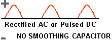
Note only the positive part of the AC cycle is present as pulses of DC
The DC pulsed is the AC rectified by the use of a single diode as previously shown above.
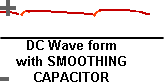
Identify the resulting waveforms.
In the section on capacitors it was explained that a capacitor can be "charged" by a DC source to the potential difference of that source. It has also been explained that a capacitor can hold a charge and can also give up a charge.
This ability to charge and discharge can be used to great effect in a simple PSU (power supply unit) when a single diode is used to rectify the AC in the secondary of a transformer.

The above simple circuit represents the transformer with the primary and secondary winding (coils / inductors) the single diode with a smoothing capacitor.
Alternate + then -
+ but with gaps
+ with no gaps
Ensure you fully understand the difference between the three waveforms shown above. Where it is shown that there are gaps these would be very small but could still be seen on an oscilloscope screen. In the last diagram above it assumes that a capacitor is now in the circuit and the gaps disappear but note the falling line between one peak and the next as the capacitor discharges due to the "load" on the output. The capacitor is supplying the current missing from the circuit whilst the transformer is in its negative part of the waveform. The deviation from the full DC potential is called "ripple".
If there was no output load then there would be no discharge of the capacitor and the line would remain at the maximum potential level.
2I2 Recall that a variable capacitance diode behaves like a capacitor when reverse biased and that the capacitance of a reverse biased diode depends on the magnitude of the reverse bias.
VARICAP or VARIABLE CAPACITANCE DIODE or VARACTOR DIODE TUNING depends upon Reverse Voltage
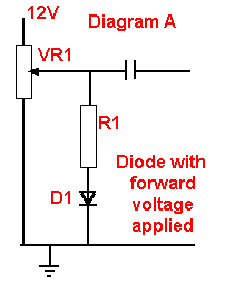
Diagram shows the normal configuration with D1 forward biased and a current would flow through VR1 into R1 and through the diode D1 to Ground.
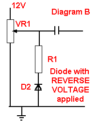
Diagram shows the REVERSED VOLTAGE configuration. With D2 reverse has a REVERSE VOLTAGE applied across it. Whilst current would pass through VR1 to ground it would not flow through into R1 due to the diode D2 preventing the flow. However this configuration gives rise to the concept that is outlined below of exhibiting the characteristics of a capacitor.
When variable capacitance diodes ( varactor diodes ) have a reverse voltage applied they exhibit the characteristics of a capacitor. Changing the applied voltage alters the amount of capacitance. Most diodes can be used but varactor diode (D1) is specifically manufactured for use in oscillator and tuned circuit.
![]() or
or
![]() D1 Variable capacitor diode
D1 Variable capacitor diode
![]() ZD1 Zener diode. You
will learn more about these in the advanced course.
ZD1 Zener diode. You
will learn more about these in the advanced course.
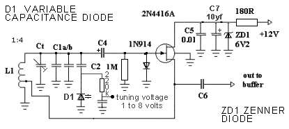
Schematic of a varactor tuned Hartley Oscillator
Both the Varicap diode and the Zener diode are types of diode. Note variation the triangular shape indicating the association with the junction diode which, is the basic diode for rectification, and is where we started at the top of this page. The Zener diode is there to stabilise the voltage to 6.2 volts.
For an oscillation to be generated, there has to be an amplifier with a loop gain in excess of 1.
This means that the random movement of electrons at the input of the amplifier is amplified, and then fed back to the input, so that the fed back signal is then even bigger, and what reaches the input again is bigger than the original random movement of electrons.
The tuned circuit is arranged such that the open loop gain of the amplifier exceeds 1 at resonance. Due to the tuned circuit being "lossy" when "off resonance", not enough is fed back. "On" resonance, little is lost, and enough gets back. The transistor amplifies this over and over until it is saturated. (i.e. fully turned on). At this point, the transistor cannot amplify and the signal is lost. No output signal = no input signal, so it all collapses. Because of the tuned circuit, what would otherwise be a square wave becomes a sine, because the tuned circuit filters out (as it is "lossy at the wrong frequency) all the harmonics. (A square wave is really a sine, with all the harmonics added to it).
So... Transistor amplifies over and over until saturated, no more output = no more input, none fed back, all collapses, then starts again. This gives a square wave and keeps "poking" energy into the tuned circuit, which removes the harmonics.
Think of a pendulum. You keep giving it a "poke" to keep it going, but it stores energy, and swings smoothly when you are not "poking" it. Important point re oscillators. They need buffer amplifiers after them, to isolate them from the load. Otherwise, changes in load will cause changes in frequency output. They also need stabilised supplies, and a mechanically rigid construction. Temperature compensation would also be common for a transmitter VFO. (A capacitor with a temperature co-efficient would be used as part of the tuned circuit. When the circuit warms up, the oscillator could drift, but the compensating capacitor alters it's value as well, and is connected such to retune the oscillator to where it ought to be.The origin of some of the text on this page is from the RSGB with additions by the web master