|
|
|||||
|
Bredhurst Receiving and Transmitting Society |
|
||||
|
|
|||||
|
3. Technical Basics 3i.5 Understand that a transistor is a three terminal device (emitter, base, collector) in which a small base current will control a larger collector current and this enables the transistor to be used as an amplifier.
Understand that the ratio of the
collector current to the base current (IC/IB)
is the current gain Note: the student is not required to recall transistor configurations. Circuits shown will be an npn transistor connected in common emitter mode. . Before we go into the syllabus fully we must take moment to describe what a transistor is and it basic operation. The
circuit diagram of an NPN transistor is:- We previously discussed the PN junction when we where looking at diodes. The transistor is called a Bipolar transistor it has 2 junctions and 3 separate connections. The transistor has a thin layer of P type material sandwiched between 2 thicker N type layers hence the name NPN transistor or bipolar transistor. The layer which forms the middle of the sandwich is called the BASE, the others are called EMITTER and COLLECTOR respectively. The transistor like the diode need forward bias to turn the transistor on and then the main current will flow through the transistor from the collector to emitter .
NPN transistor used as an AUDIO amplifier Transistor biased on by R1/R2. To compensate for changes in:
Then R4 is used to provide 100% negative feed feedback at DC. The reason this works, is because if the transistor takes more collector current, then this current passes through R4, and a bigger voltage would appear across it as a result. This voltage opposes the bias voltage that is set by R1/R2, and thereby stabilizes the transistor against changes as in 1) to 3) above.
3i.6 Understand that if the variation in the base current is large enough the collector current can be turned on and off and the transistor behaves as a switch. NPN transistor used as a switch
Here, we are not concerned with amplification of a signal such that we want a faithful (and larger) reproduction of the signal on the output of the transistor. We need DC stability (i.e. the transistor should stay "off" when intended, and not be affected by transistor type variations, temperature, or supply voltage). We also need the transistor to turn fully "ON", again not affected by the above variations. This is fortunately simple; we have only to ensure that there is a resistor connected between base and emitter (R3) to ensure it is held "OFF", and then apply, via a resistor (R1), some current to the base. What we apply needs to be enough to ensure that the transistor is fully turned on despite variations as above, and also be enough to allow some to go through R3, (This resistor "nicks" it from the transistor!). The on and off concept according to the configuration. Ask your tutor to build a small circuit based upon the above so that you can see the difference between the two circuits in that sometime applying a current to the base turns the led on and sometimes it is the other way round that applying a current turns the led off. Understand that the ratio of the collector current to the base current (IC/IB of the transistor. A
Transistor is a current amplifying device. So if the base current Ib is 10uA and the collector current Ic is 1mA Beta = 1mA/10uA = 100 If transistor has a Beta of 200 and the bases current Ib is 100uA then the collector current would be 200 times greater or 3i.7 Recall that a transistor must be provided with the correct DC voltages and currents to allow it to function and that this is termed correct biasing. Note that calculations are not required. For a transistor to work correctly as an amplifier the correct proper potential voltage must be present on base, collector and emitter so the transistor is biased to achieved this. Normally the term bias refers to the voltage applied to the base to bring the operating point to a linear part of the transistor amplification curve . For a Germanium transistor a voltage between emitter and base of 0.3 volts and for a silicon transistor 0.6 volts.
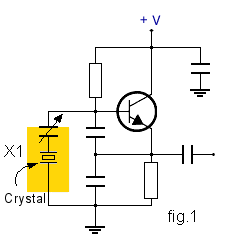
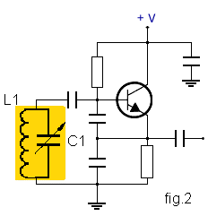
3i.8 Recall that a transistor can be used to generate audio and radio frequencies by maintaining the oscillations in a tuned or frequency selective circuit. A simple fact to be recalled is that a transistor can be used as an oscillator to generate audio and radio frequencies. The sort of question you might be asked in this section is what can a transistor be used for of which 3 will be spoof answers. Distinguish between a crystal oscillator and a variable frequency oscillator (VFO) based on a tuned circuit. Diagrams will show the Colpitts oscillator with the transistor in emitter follower mode. Students are not expected to recognise other types of oscillator. The above are not practical circuits as no off bias exists to the transistor BUT the important parts to recognise are those that have been highlighted. The diagram fig.1 on the left shows a crystal and thus is a fixed frequency Crystal Oscillator. Do not be confused with the variable capacitor into thinking that it is a variable oscillator as the variable capacitor is there to bring the crystal oscillator to resonance at a particular frequency. sometime the variable capacitor is not even in the circuit. The diagram fig.2 on the right shows a tuned circuit highlighted and also shows a variable capacitor in parallel with an inductor, making up the tuned circuit, and thus is a variable frequency oscillator.
The advantage of using a coil and a capacitor to determine the required frequency is that either component may be varied to alter the frequency. It is not difficult to alter these components, and variable types are available. The down side of doing so is that a number of things (like a change in temperature) can cause the actual value of the coil, or the capacitor to vary, and as a result, the frequency changes. |
|||||
|
|
|||||
|
|
|||||
|
|
|||||