|
|||||||||||||
|
|
|
||||||||||||
|
|
|||||||||||||
|
Syllabus Sections:- --------------------------------------------------------------------------------------------
2J2 18 Understand the function of stabilising circuits and identify different types of stabilising circuits (i.e. Zener diode/pass transistor and IC) Note: questions on the characteristics of individual components are covered earlier in this syllabus, e.g. This sub-section is on complete circuits.
The Regulation must be able :-
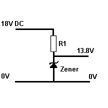
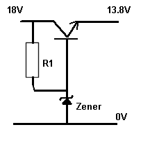
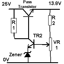
Stabilising circuits / REGULATION The other part that is needed is some form of REGULATOR to keep the output voltage at say 13.8V all the time without any regard as to the level of current being drawn. In its simplest form, for low current use, a regulator could be as simple as a Zener diode and a resistor in series across the DC supply. The value of the zener diode determines what the output voltage is. The next stage would be to add a pass transistor as shown below. Here again the zener determines the output voltage. The next stage in complexity would have a regulator which consists of a few more components as shown in the diagram below as it develops. In this case it is the variable resistor as part of the potential divider chain of resistors that determines the output and thus can be "set" to the output required. The transistor at the top is called a PASS TRANSISTOR as it is passing all the current going to the output terminal. The lower transistor is part of the regulator circuit. Please note a ZENER diode has been used at a voltage of 5.6V. Such a rated diode performs very well and can control the voltage close to 5.6V without change due to heating. With the power turned on the preceding part of the circuit will supply 25V to the collector of the pass transistor. R1 will then supply a small current to the base of the pass transistor and current will then flow through the transistor to the output terminal where the diagram is marked 13.8V. -------------------------------------------------------------------------------------
The 13.8V is controlled by the potential divider chain of R2 and VR1 which controls the current flowing into the base of the second transistor. If the 13.8 goes higher then more current flows into the base turning TR2 on harder. This results in there being less current available to the base of the pass transistor, hence the output falls to a point where there is equilibrium in the circuit. The zener is always conducting, providing a reference voltage against which the output voltage is compared. If the 13.8V goes lower then less current flows into the base and TR2 begins to turn off. This results in there being more current available to the base of the pass transistor, turning it on more, and the output voltage rises to the point where again there is equilibrium in the circuit. This action continues and thus regulates the output voltage and stabilizes it to 13.8V +/- a very little. VR1 is used to set the output level at 13.8V initially. The use of an IC It is possible to carry out many of the above functions with an IC such as LM723 which is a voltage controlling IC. Discussion in the course is not required other than to be aware that IC's can control voltage circuits of a power a supply when used in conjunction with pass transistors and other components.
PEAK INVERSE VOLTAGE
|
|||||||||||||
| 2J4 18 Understand the
basic principles and operation of a switch mode power supply,
at block diagram level The block diagram concept was introduced to you at Foundation Level as it only shows the blocks of parts which make up the whole unit and does not go to component level.  ,
you can see that the mains supply in the diagram above, is
on the left hand side and this enters an "Input Filter"
which takes out any spurious electrical noise which may be
generated in the power supply from going back in to your
mains supply in your property. Such a filter is present in a
good quality switch mode power supply. ,
you can see that the mains supply in the diagram above, is
on the left hand side and this enters an "Input Filter"
which takes out any spurious electrical noise which may be
generated in the power supply from going back in to your
mains supply in your property. Such a filter is present in a
good quality switch mode power supply.The mains AC voltage is fed into a "Rectifier Circuit" to provide High Voltage DC, and as in a traditional power supply with a transformer there will normally be a reservoir capacitor following the rectification. The next part is a "Chop" comprising of high voltage transistors acting as switches on and off, which chops up the DC into short pulses at around 30 to 60 kHz. As these transistors are either on or off, the power dissipation is low compared to the traditional power supply switching transistors. The pulses are then fed into a "Transformer" which converts the high voltage pulses to pulses of the required voltage, which it passes to the next stage. As the transformer is dealing with relatively high frequencies compared to the usual 50Hz supply, the transformer in a Switch Mode Power Supply can be much reduced in size. Also the Transformer has a Ferrite Core and not a Soft Iron so that the core does not become "saturated" and stop working. The winding of the transformer are also well insulated. After the Transformer stage is another "Rectifying Circuit" which converts the High Voltage DC to Low Voltage DC. The regulation of the DC pulses to the required voltage is achieved by looking at (or in electrical terms "Sampling") the output voltage of the pulses, and comparing the pulses via an opto-isolator (also know as an opto-coupler), to control "The CHOP" of the pulses' width on the primary side of the transformer. A smoothing capacity will exist after the second rectification block diagram and this capacitor can be much smaller than in the conventional power supply because it is working at higher frequency of about 50kHz. Making sure the OUTPUT voltage is as required there is a feed back circuit through an opto coupler which acts to isolate the signal but passes the pulse width to the primary side of the transformer.
Whilst the whole unit is much smaller than the
conventional power supply it does have a down side, it
can create harmonics due to the switching.
In
the block diagram the "Input filter" to stop the
harmonics leaking into the mains supply and an other
"Output Filter" ensures that no harmonics go into the
low voltage supply to your equipment. Such
filters are present in a good quality switch mode
power supply. Failure to
have good filtering and screening can create high
background RF noise which would be picked up on your
radio receiver.
Here
is a picture of a typical Switch Mode Power Supply
 |
|||||||||||||
|
|
|||||||||||||
|
|
|||||||||||||
|
|
|||||||||||||